
Simple Radio PCB - slow progress
- Aurash

- Mar 8
- 1 min read
it's been a while since I posted any progress on this project, I got some PCBS made and paste stencil, purchased the parts and ...I got busy with other stuff, story of my life.
The basic schematics is done, and I'll do my best to build one/two boards soon.
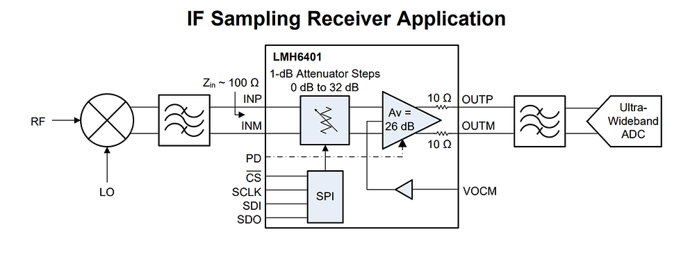
The PCB looks deadly, I made the choice to have a SMA connector between the VGA (variable gain amplifier) and the ADC for testing the analog part without the digital part. (divide and conquer)
For powering the board I brought V+,V- and VCM (common mode voltage) pin to a connector for making experiments.
VOCM can be set with a resistive divider or can be supplied using the connector (and not populate the two resistors) - see the schematics below
This board resembles more an evaluation board than an actual project, but that's the main purpose (to clear some of my design insecurities) - buying eval boards for all the ICs that I used was a bit expensive and having the scmeatics and pcb design for further development was required anyway.

Schematics are available to download
Pictures of the actual PCB below. I'm not decided if I'm going to assemble this on the pick & place machines or just make them by hand
Actual picture with the PCB

I'm looking forward to assemble this and test it so I can switch back to FPGA side of the project.
Have Fun, see you soon.


Comments